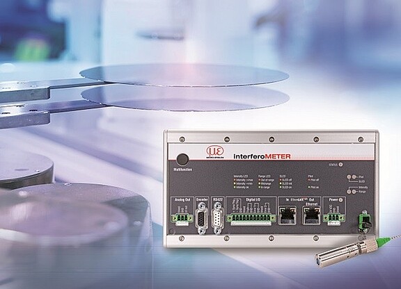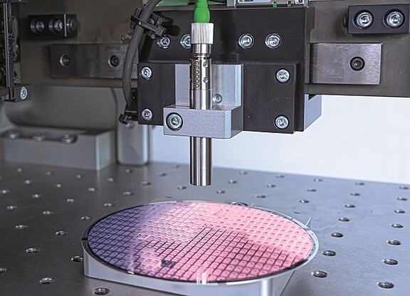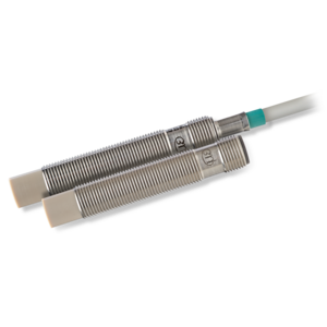

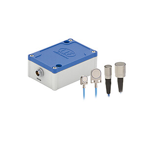
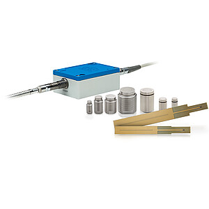
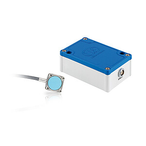
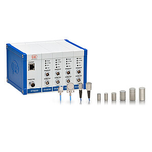
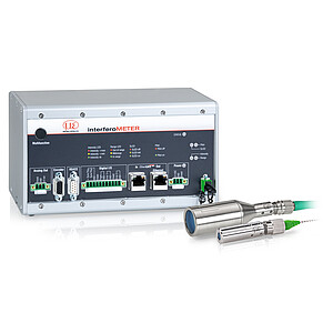
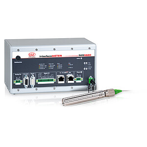
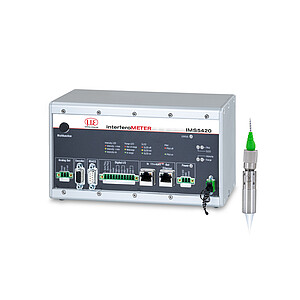
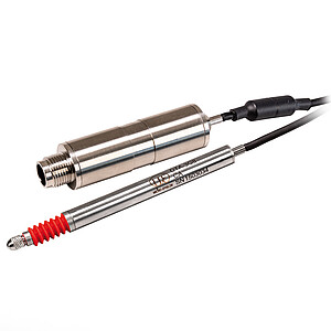
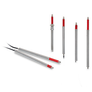
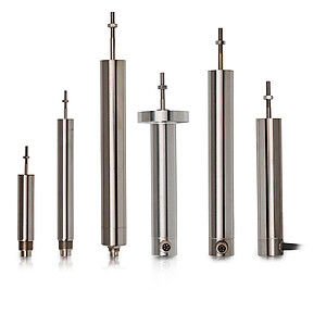
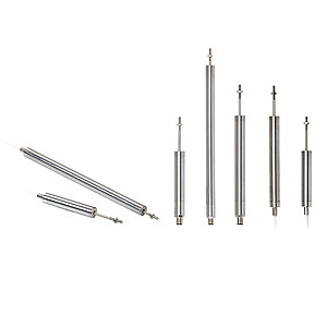


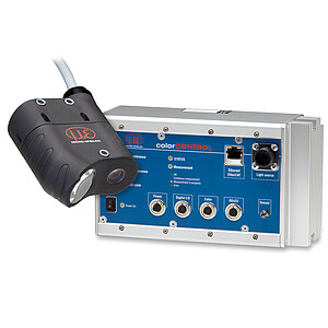
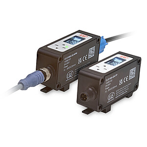
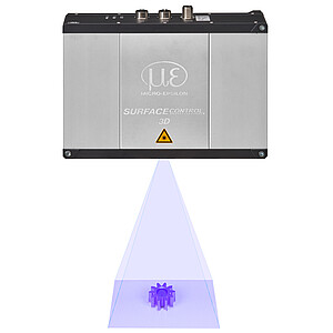


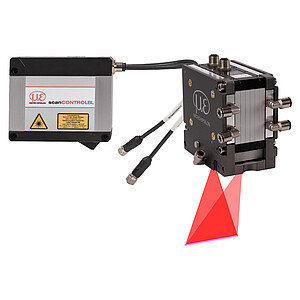
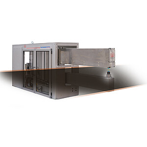
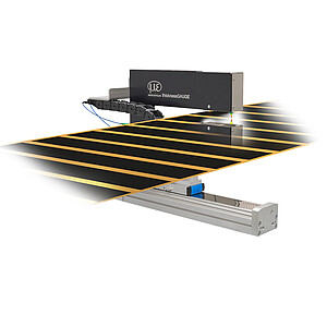
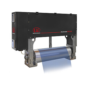


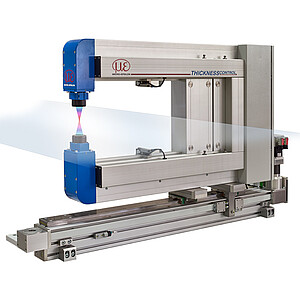

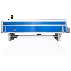


In semiconductor production, high precision is essential. A critical stage is the lapping of the blanks, which ensures a uniform thickness. In order to continuously monitor the wafer thickness, white light interferometers are ideally suitable, says Glenn Wedgbrow, Business Development Manager at Micro-Epsilon UK.
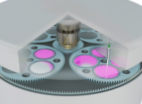
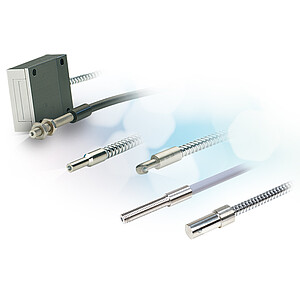
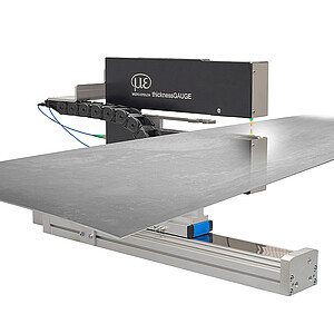
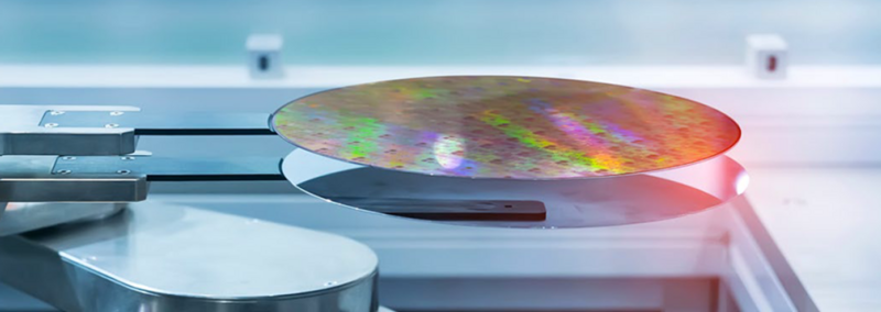
Many process steps are required before semiconductor chips can be made from silicon. First, slices around one millimetre thick are cut from a crystalline silicon ingot, which are then lapped. This gives them the desired thickness and surface quality. Only then can semiconductor chips be manufactured from the wafers using further processes.