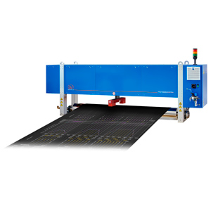
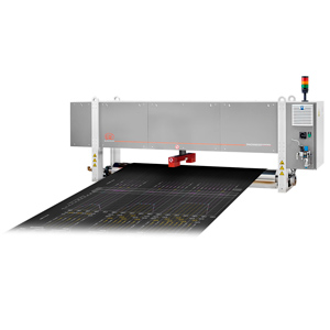
Another application in PCB manufacture is the scribing of pre-determined breaking points into the panels for de-panelling. A PCB consists of several panels or smaller PCBs that go through production as one large PCB. This kind of bundling is necessary for production reasons as it makes boards easier to assemble. The scribe lines are normally produced by two opposing saw blades that cut a V-groove into the board, which allows small PCBs to be easily and cleanly de-panelled (i.e. separated from one another) by the end of the production processes. The scribe lines are around 400 µm wide.
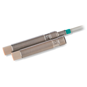
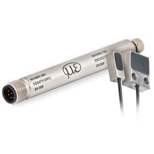
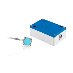
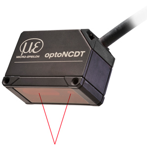
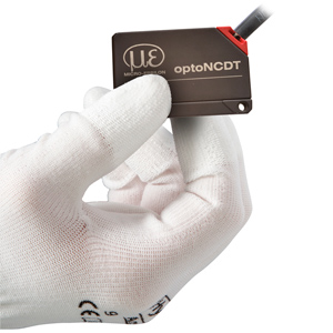
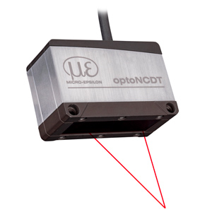
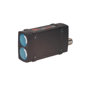
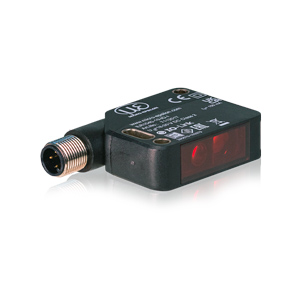
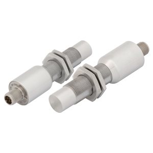
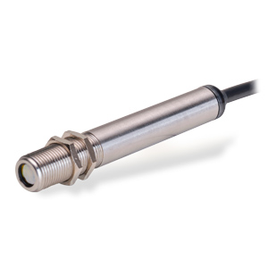
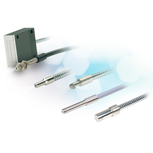
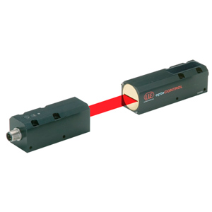
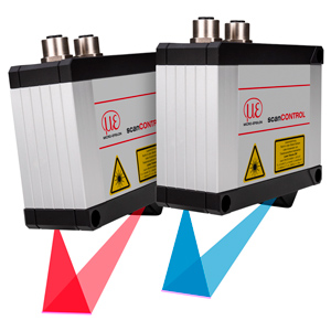
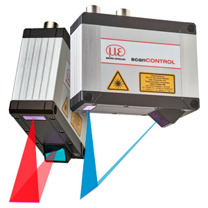
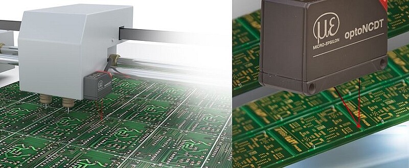
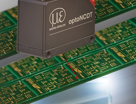
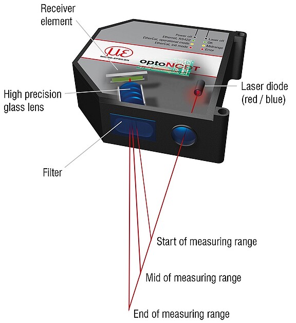
The scribe lines of PCB panels must be measured precisely. Here, the optoNCDT 1420 laser sensor is also used due its unique combination of speed and precision combined with an extremely compact design. During production, the sensor detects whether the keyway is accurately milled into the panels. If the scribe line is too thin, the panels will break during the production process, which consumes resources and may cause damage to the machines. If the grooves are not milled deeply enough, the panels would fray during de-panelling and break irregularly, which means that they would not fulfil the quality requirements resulting in waste.
Conclusion
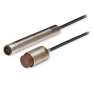
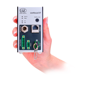
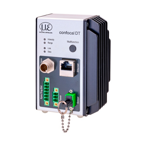
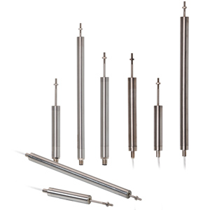
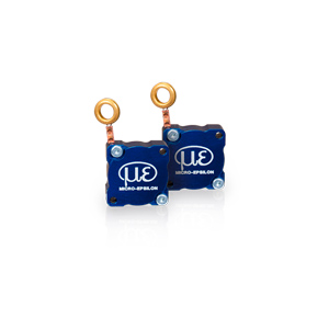
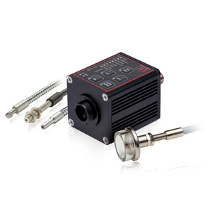
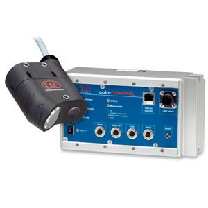
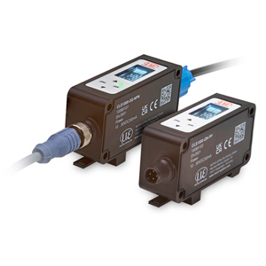
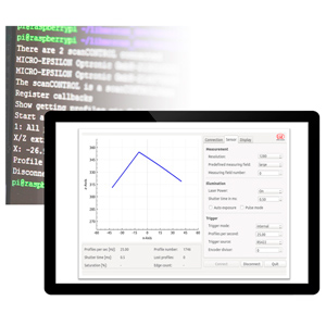
Using modern sensors such as the optoNCDT 1420 laser triangulation sensor from Micro-Epsilon helps to improve quality while reducing waste and saving money. The laser sensor reliably measures displacement, distance and position with repeatability from 0.5 µm. Its extremely small measurement spot accurately detects even the smallest of PCB components such as IC pins. With up to 8,000 measurement values per second, the sensor is designed for highly dynamic processes such as those found in the electronics industry and additive manufacturing. A compact design with integrated controller simplifies integration in machines and systems even where installation space is tight. Intelligent surface control balances the fluctuating intensity of the light reflected during the measurement process when colour or brightness change rapidly. Particularly with PCBs – where matt and shiny, as well as bright and dark objects are side by side – this is a major advantage in order to achieve stable and micrometer-accurate results. The intuitive web interface allows the user to configure the sensor and offers predefined presets for different measurement tasks. Furthermore, up to eight user-specific settings can be stored and exported. The video signal display, signal peak selection and a freely adjustable signal averaging, enable the measurement task to be optimised. The region of interest (ROI) function allows, for example, interference signals to be filtered out. Fast commissioning is also possible.
For more information, please visit www.micro-epsilon.co.uk or call the Micro-Epsilon sales department on +44 (0)151 355 6070 or email info@~@micro-epsilon.co.uk