Planarity testing in hybrid bonding
"Hybrid bonding" is an advanced connection technology in semiconductor production in which two wafers or chips (dies) are directly connected to each other via copper contact surfaces. This eliminates the need for conventional solder balls. In modern die-to-wafer (D2W) or wafer-to-wafer (W2W) hybrid bonding, real-time planarity measurement is the decisive factor for a reliable process.
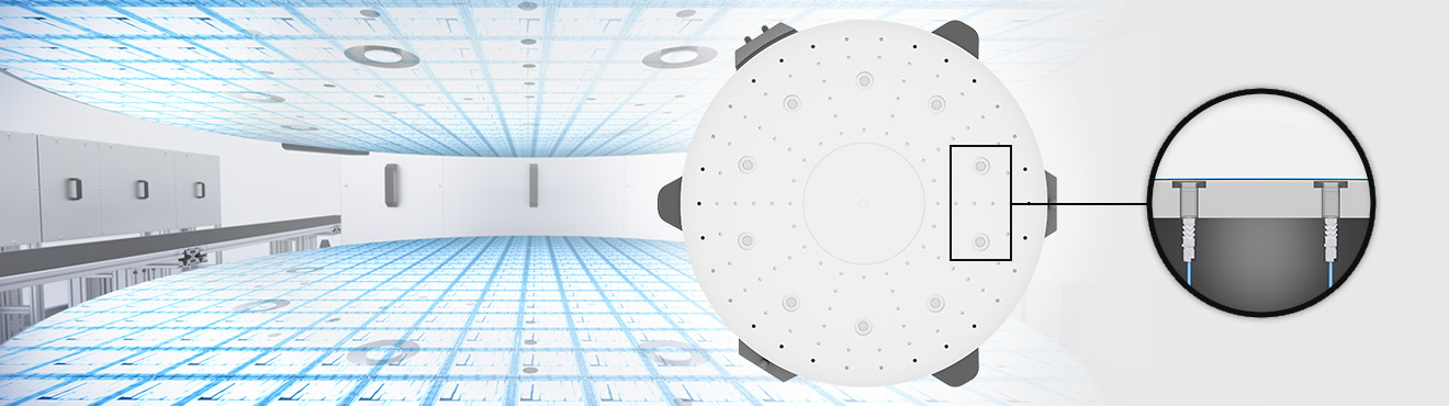
Capacitive distance sensors play a central role here, especially for small chips with fine structures in the micrometre range. They enable the non-contact measurement of shape deviations on wafers - for example due to deflection, twisting or local distortion. In this way, the sensors monitor the planarity of the wafers and provide essential measurement data for adaptive leveling of the bonding units.
Inline planarity control before bonding
Depending on the measurement task, sensor arrays scan the surface of the upper and lower wafer and detect local elevations, depressions, inclinations or the entire deflection. The measurement data flows into an active position correction of the wafer stages. If height differences are detected, the bonding unit can be precisely aligned in the z-axis direction using a precision axis, for example. For very small chips, segmented areas on the chuck are also used, which can be leveled locally.
The capacitive sensors continuously supply measurement data with the highest precision, enabling the bonding systems to be controlled via actuators (e.g. Piezo actuators or segmented bond chucks) in real time.
Thanks to their vacuum-compatible design, these sensors can be used in almost all fields of application.