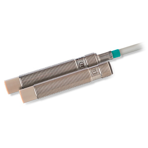
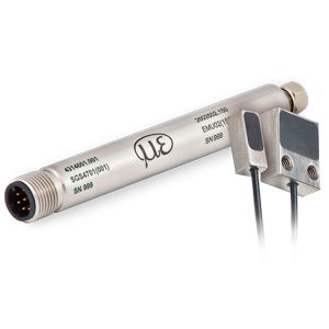
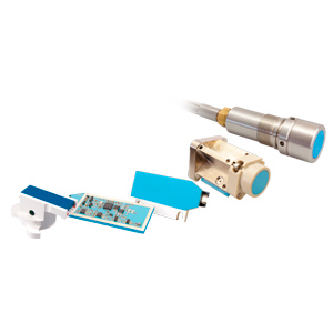
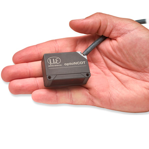
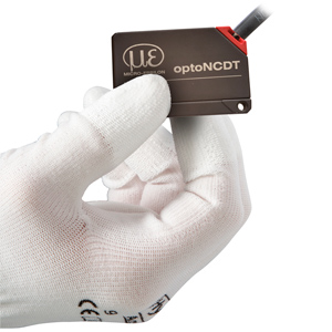
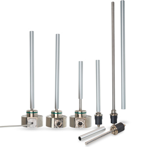
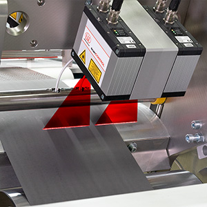
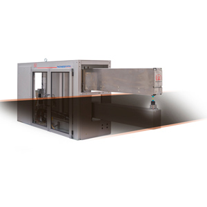
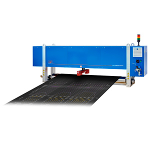
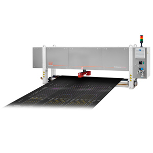
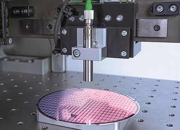
The new range of interferometers from Micro-Epsilon for measuring the thickness of wafers have already been extensively tested in reference projects in the semiconductor industry. Even challenging applications were mastered: in the lapping machines, the devices measure reliably even when there is liquid with the cutting grains on the wafer surface. The cleanroom variant uses Micro-Epsilon’s own cleanroom technology, which enables cleanroom-compatible packaging of the components, for example.
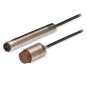
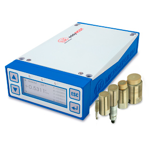
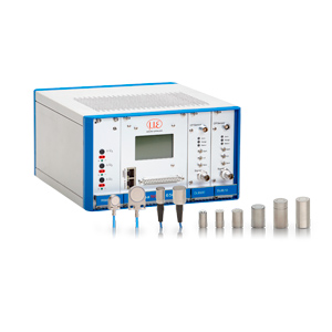
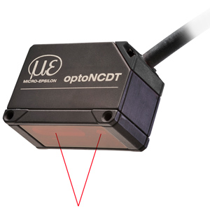
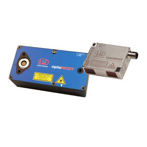
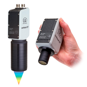
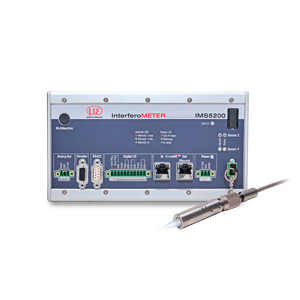
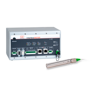
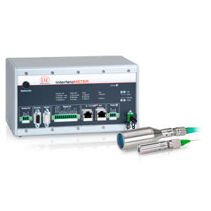
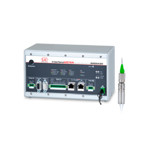
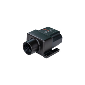
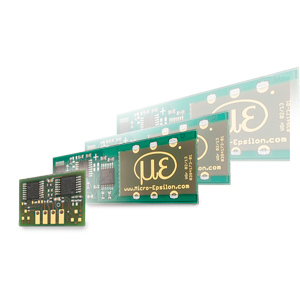
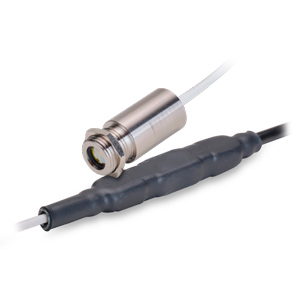
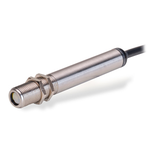
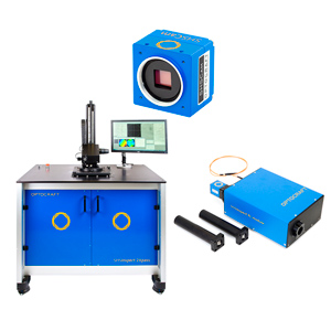
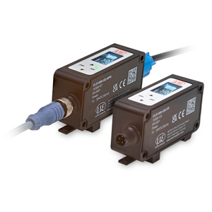
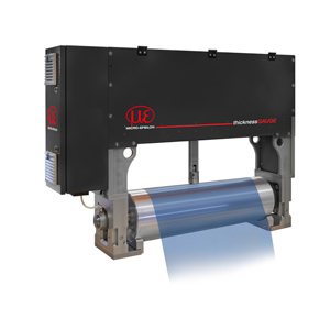
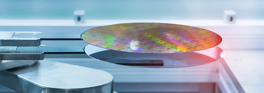
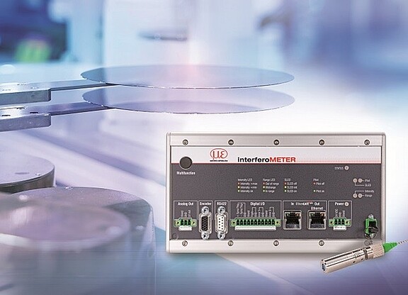
The IMS5420-TH white light interferometer opens up new perspectives in industrial thickness measurement of monocrystalline silicon wafers. Due to its broadband superluminescent diode (SLED), the IMS5420-TH can be used for undoped, doped and highly doped SI wafers. In wafer thickness measurements, the IMS5420-TH impresses with an excellent price/performance ratio.
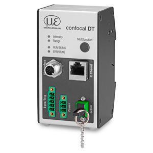
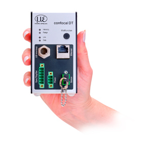
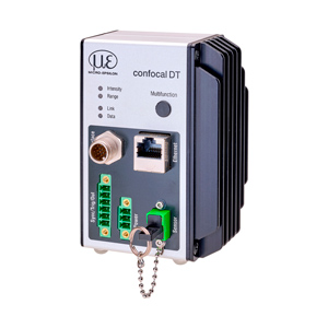
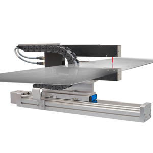
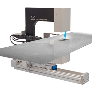
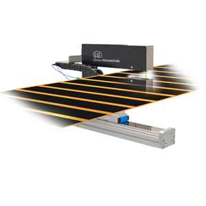
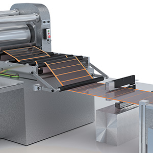
The white light interferometer achieves a signal stability in the sub-micrometre range. The thickness can be measured from a distance of 24 mm. The measuring system is therefore ideally suited for inline measurements.
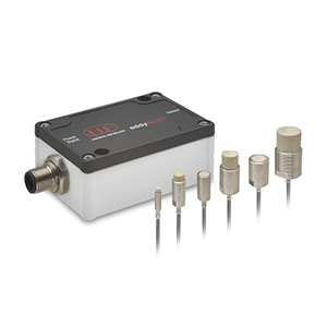
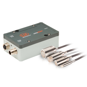
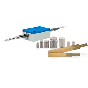
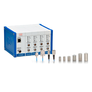
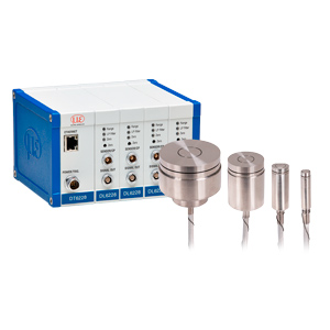
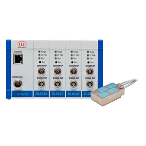
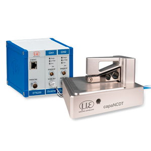
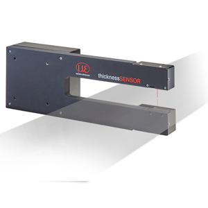
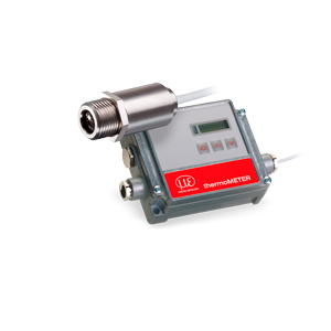
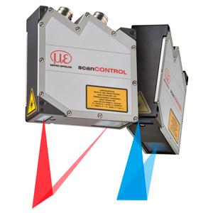
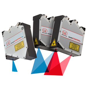
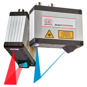
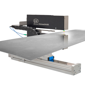
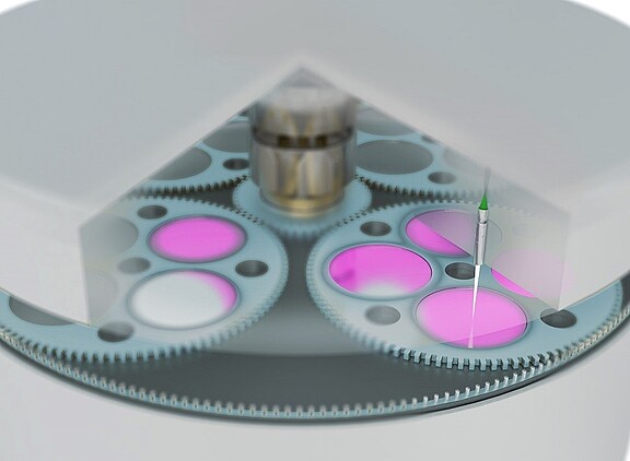
The measuring system is available as a thickness measuring system or as a multi-peak thickness measuring system. The multi-peak system measures thicknesses of up to five layers, for example, wafer thickness, air gap, films and coatings.
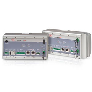
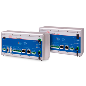
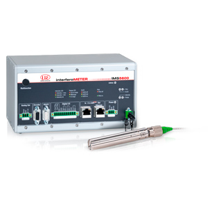
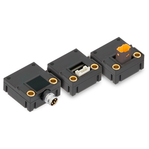
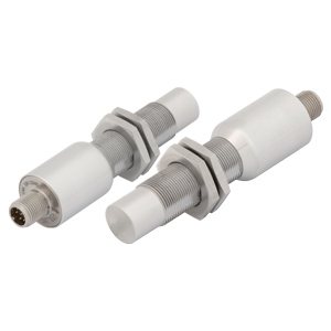
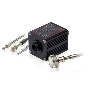
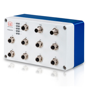
In addition to silicon wafers, the IMS5420 also precisely detects the thickness of silicon carbide wafers. For thickness measurements in harsh environmental conditions, the IMS5420/IP67 controller is available with IP67 protection and stainless steel housing.
For more information, please visit www.micro-epsilon.co.uk or call the Micro-Epsilon sales department on +44 (0)151 355 6070 or email info@~@micro-epsilon.co.uk