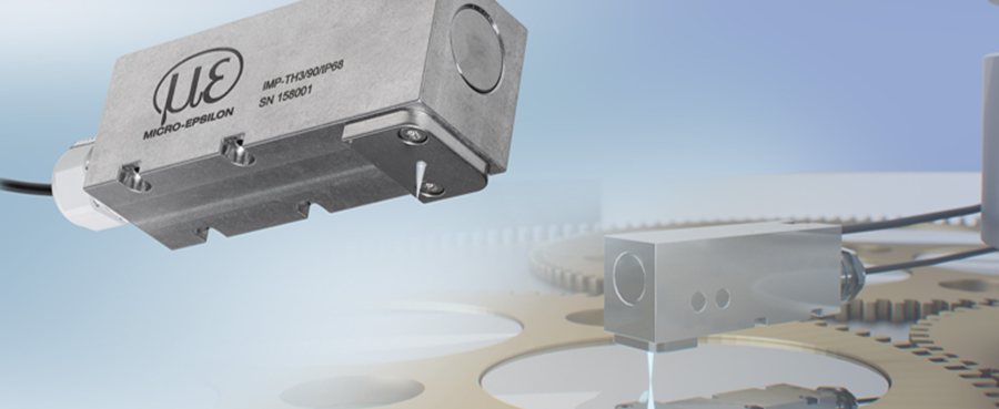
Precision sensor supplier Micro-Epsilon has further developed its interferoMETER range of white light interferometers to include a sensor with a 90° beam path that enables stable thickness measurement of silicon and silicon carbide semiconductor wafers.
With a 90° beam path, IP68 protection rating and integrated air purge device, the new robust interferoMETER IMP-NIR-TH3/90/IP68 is specially designed for demanding production environments. The sensor enables precise thickness measurements of semiconductor wafers during production – even when high particle loads occur such as in the slurry grinding process. The sensor has a small working distance of just 3 mm, making it ideal for applications with very limited installation space.
Stable measurements in grinding processes
The sensor shows its strengths particularly in demanding processes such as slurry grinding. The robust IP68 stainless steel housing allows it to be used directly in the machine, even with high humidity and high particle loads. In grinding and lapping processes, a clean appearance is critical. This is ensured by the integrated air purge device, which keeps the optics permanently free of particles, which enables stable measurements.
90° beam guidance for confined installations
A key feature of the sensor is the 90° optical beam path, which enables integration in very tight installation spaces. The working distance (3 mm) and very small light point diameter (15 μm) create the basis for high precision inline measurements directly in the machine. The IMP-NIR-TH3/90/IP68 sensor is operated using the IMS5420 controller, providing a compact, reliable solution for the measurement of highly doped wafers, where high signal quality is critical.
The interferoMETER IMS5420 system incorporates a broadband superluminscent diode (SLED) with a wavelength range of 1,100 nm, allowing thickness measurements of undoped, doped and highly doped silicon wafers using only one measuring system. Thicknesses from 50 to 1050 µm can be measured with a doping of up to 5 mΩ cm from a distance of 24 mm and signal stabilities (z-axis resolution) of less than 1 nm can be achieved. Even for highly doped wafers with a specific resistance of 0.005 Ω cm, thicknesses from 0.05 mm to 0.85 mm can be measured.
With a measuring rate of up to 6 kHz, the interferoMETER IMS5420 is suitable for in-line and at-line thickness measurements, for example, after and during grinding and lapping, as well as during quality control. Other applications for the measurement system include thickness measurement of glass and film.
Multi-layer thickness measurements
The interferoMETER IMS5420 is available either as a thickness measuring system or as a multi-peak (MP) version for thickness measurement of up to five layers (e.g. wafer thickness, air gap, film and coatings > 50 µm) with silicon thicknesses from 0.05 to 1.05 mm. The measurable thickness of air gaps is up to 4 mm.
For easy set up and configuration, a modern, intuitive web interface is provided. In addition, various interfaces (EtherCAT, Ethernet, Profinet, EtherNet/IP, RS422, analogue) offer numerous integration options.
For more information on the interferoMETER IMP-NIR-TH3/90/IP68, please visit interferoMETER 5420-TH | Micro-Epsilon or call the Micro-Epsilon sales department on +44 (0)151 355 6070 or email info@~@micro-epsilon.co.uk